
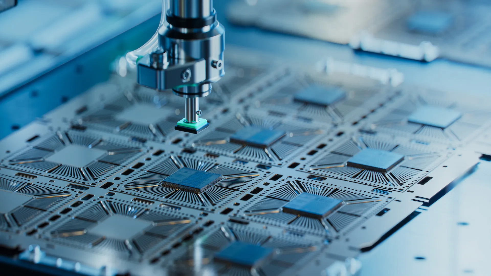
The rapid evolution of consumer electronics has been defined by a singular, relentless trend: the drive toward miniaturization. As our devices become smaller, thinner, and more powerful, the traditional methods of shaping metal components have struggled to keep pace. While mechanical stamping and laser cutting are effective for many industrial applications, they often fall short when dealing with the microscopic tolerances required for high-end electronic hardware. This is where chemical milling, also known as photochemical machining or chemical etching, emerges as a cornerstone technology. By using controlled chemical reactions to remove material, this process allows manufacturers to create intricate metal parts with a level of precision and stress-free consistency that physical tools simply cannot replicate.
Understanding the Fundamental Process
Chemical milling is a subtractive manufacturing process that uses a chemical solution, known as an etchant, to dissolve unwanted material from a metal substrate. Unlike traditional machining, which relies on physical force to gouge or cut through metal, chem mill is a non-contact method. The process begins with a sheet of metal that is thoroughly cleaned and coated with a light-sensitive polymer called a photoresist. A photographic film, or mask, containing the desired design is placed over the coated metal and exposed to ultraviolet light. The light hardens the resist in specific areas, while the unexposed areas remain soft and are washed away during the development phase.
Once the protective mask is in place, the metal sheet is sprayed with or submerged in a heated chemical etchant. The chemical selectively attacks the exposed metal surfaces, dissolving them atom by atom until the desired shape or depth is achieved. Because the etchant works uniformly across all exposed areas simultaneously, the complexity of the design does not increase the time or cost of production. This makes the process ideal for creating parts with thousands of tiny holes, complex geometries, or ultra-thin profiles that would be impossible to manufacture using mechanical drills or punches.
Eliminating Mechanical Stress and Burrs
One of the most significant advantages of chemical milling in the electronics industry is the absence of mechanical stress. When a metal part is stamped or cut with a blade, the physical impact creates internal stresses and can cause the material to warp or deform. Furthermore, mechanical cutting often leaves behind burrs, which are small, jagged edges of displaced metal. In the world of high-frequency electronics and printed circuit boards, even a microscopic burr can lead to a short circuit or interfere with the flow of a signal.
Chemical milling avoids these issues entirely. Because the material is dissolved rather than cut, the edges of the finished parts are perfectly smooth and free of burrs. The molecular structure of the metal remains undisturbed, ensuring that the physical properties of the component, such as its conductivity and magnetic permeability, are preserved. For manufacturers of sensitive components like lead frames for integrated circuits or electromagnetic interference shielding, this stress-free environment is essential for ensuring the long-term reliability and performance of the device.
Sustainability and Future Outlook
As we look toward the future of manufacturing, the electronics industry is increasingly focused on sustainability and reducing its environmental footprint. While chemical milling involves the use of corrosive substances, modern facilities have implemented sophisticated recycling and regeneration systems. These closed-loop systems allow the etchant to be cleaned and reused multiple times, while the dissolved metal can be recovered and sold as scrap. This reduces waste and lowers the overall environmental impact of the process compared to traditional machining, which generates large amounts of metal chips and requires cutting oils.
The role of chemical milling in electronics is only set to expand as we enter the era of flexible electronics and wearable technology. The ability to etch patterns into ultra-thin foils and flexible substrates opens up new possibilities for sensors, medical devices, and foldable screens. By combining the precision of chemistry with the speed of photographic imaging, chemical milling remains an indispensable tool for engineers pushing the boundaries of what is possible in the digital age. It is a silent but essential partner in the creation of the devices that define our modern lives.


More Stories
Future Horizons: The Next Big Leap in Mobile Trends
Pioneering Tomorrow: How 5G is Reshaping Innovation Across Industries
Unleashing the Power of 5G: A New Era of Connectivity and Innovation